- Címlap
- LED kijelzők meghajtása
- Permetező projekt
- PIC18FxxK42
- PIC18FxxK42 I2C regiszterei
- PIC18FxxK42 órajel beállítása
- Pic18FxxK42 regiszterei
- Láb hozzárendelés PIC18FxxK42
- Pic18 I2C programozás
- PIC18FxxK42 I2C kommunikáció
- EEPROM memória használata
- LIN UART-tal fordítás
- LM75A és PIC18F45K42 I2C1 program
- Objektumok
- Pic18FxxK42 konfigurálás
- SPI
- UART PIC18(L)F45K42
- Watchdog Timer
- PIC18F45K42 timer2,-4,-6
- I2C modul 1
- PIC18F45K22 I2C lépései
- PIC18F45K42 USART regiszterei és azok magyarázata II.
- PIC18F45K42 USART regiszterei
- PIC18F45K42 timer1,-3,-5
- UART PIC18F45K42
- PIC18 utasításkészlete
- USART mudullal aszinkron kapcsolat két mikrokontroller közt
- CAN kommunikáció
- DS3231SN RTC
- Dell T 5600
- E-paper
- EGYÉB jegyzet
- ESP 8266 WiFi modul
- ESP-07 ESP-12x
- ESP-12F WiFi modul
- ESP32
- ESP8266
- Egyéb (elektronika)
- Emeléskijelző projekt
- Giroszkóp
- HASZNOSAK
- Hasznos általános linkek
- Illesztő modulok
- Kapcsolások, megoldások
- Kiszajú műveleti erősítő
- Konfigurálás
- LIN kommunikáció UART-tal
- MPASM PIC18
- Nyomásmérés MS5803-05BA-val
- Nyomásmérő I2C
- Nyomásszenzor SPD8xx I2C
- Nyák, nyáktervezés
- Operációs rendszerek
- PIC 18 mikrokontrollerek
- PIC18(L)F47K40
- PIC18(L)F65K40
- PIC18F45(K)50
- PIC18F87k22(80 láb)
- PROGRAMOZÁS
- Programozás
- Python 3
- RAUCH 2057153
- RDS
- RTC TLC 5947-el
- Rádiókapcsolat két mikrokontroller között
- Számítógépes programok
- TCS34725 színérzékelő
- TLC 5947
- TTP223 kapacitív nyomógomb
- USB + USB AN1310-el
- Ulefone Power 2
- Vektoros megszakítások
- Vetőgép
- Webfejlesztés
- WiFi, Bluetooth modulok
- Pickit 3 programozó
- Pic-Ethernet-Pic
- LM75A
- PWM CCPx modullal
- PWM PWMx modullal
- NCO
- TCS 3200 RGB érzékelés
- Nyáktervezés
- Oktatás
- PIC 24 mikrokontrollerek
Érdeklődési kör: elektronika, programozás, mikrokontroller programozás
I2C modul
Adatlap (pdf): PIC18F(L)xxK42.pdf
I2C kommunikáció (Eng.): Itt
I2C kommunikációban használt regiszterek: Itt!
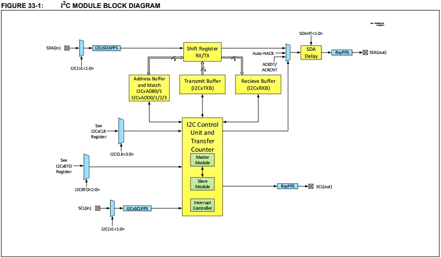
| 33.0 I2C MODUL Az adott mikrokontrollernek két dedikált és független I2C modult tartalmaz. A 33-1. Ábra az I2C interfész modul blokkdiagramja. Az ábra mind a Master, mind pedig a Slave módot együtt mutatja. |
33.0 I2C MODULE The device has two dedicated, independent I2C modules. Figure 33-1 is a block diagram of the I2C interface module. The figure shows both the Master and Slave modes together. |
||||||||||||||||||||||||||||||||||||||||||||||||||||||||||||||||||||
 |
|||||||||||||||||||||||||||||||||||||||||||||||||||||||||||||||||||||
| 33.1 I2C jellemzői • Az IC-be bele integrált I2C aramköra következő módokat támogatja: - Master üzemmód - Szolga üzemmod NACK jel értelmezésével. (NACK= Mester nyugtázó jele a mester megfelelő adatfogadáskor a szolgától) - Multi-Master (Több mester) üzemmod • Dedikált címzési-, adatfogadó-, adatldés tároló megvalósítása külön regiszterekkel • Legfeljebb négy Slave cím illesztése. • Általános híváscímek illesztése (azonosítása) • 7 bites és 10 bites címzés maszkolással • Start, Restart, Stop, Address (címzés), Write(írás), és ACK jel esetén megszakítás lehetőséggel • Órajel (szinkronjel) nyújtás ha: - RX Buffer (adatfogadó adattárolója) tele van - TX Buffer (adatküldő adattárolója) üres - Címzés után, írás és ACK jel után • Busz jelütközés érzékelés a sorrendiség kezeléséhez • Busz időtúllépés érzékelése • SDA tartási idő megadása •I2C, SMBus 2.0, és SMBus 3.0 bemeneti szint kiválasztása |
33.1 I2C Features • Inter-Integrated Circuit (I2C) interface supports the following modes in hardware: - Master mode - Slave mode with byte NACKing - Multi-Master mode • Dedicated Address, Receive and Transmit buffers • Up to four Slave addresses matching • General Call address matching • 7-bit and 10-bit addressing with masking • Start, Restart, Stop, Address, Write, and ACK Interrupts • Clock Stretching hardware for: -RX Buffer Full - TX Buffer Empty - After Address, Write, and ACK • Bus Collision Detection with arbitration • Bus Timeout Detection • SDA hold time selection •I2C, SMBus 2.0, and SMBus 3.0 input level selections |
||||||||||||||||||||||||||||||||||||||||||||||||||||||||||||||||||||
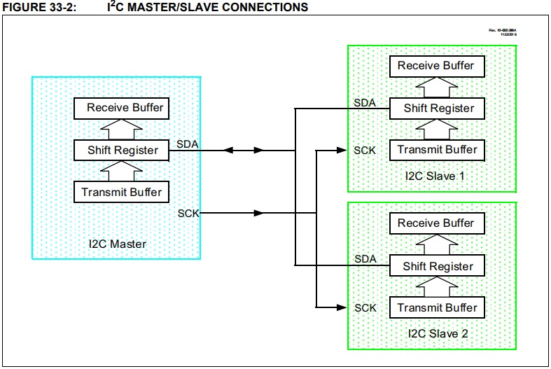
| 3.2 I2C Modul ismertetése Az I2C modul szinkron interfészt biztosít a mikrokontroller és az I2C-kompatibilis eszközök között a kétvezetékes I2C soros busz használatával. Az eszközök master/szolga kapcsolatban kommunikálnak. Az I2C busz két jelvezetéket tartalmaz: • Soros órajel (szinkronjel) (SCL) szál vagy vezeték • Soros adat (SDA) szál vagy vezeték Mind az SCL, mind az SDA vezetékek minfkét irányban nyitott kollektoros ki/be menetek, ezért az SCL is és az SDA vonalak is felhízó ellenállást igényelnek a pozitív tápfeszültséghez. A vonal lehízását logikai zérusnak tekintjük, és a vonal felengedését logikai egynek tekintjük. Az I2C busz minden tranzakcióját a Mester kezdeményezi és a szinkronjelet is ő szolgáltatja. A 33-2 ábra tipikus kapcsolódást mutat a mester és egynél több slave között. |
3.2 I2C Module Overview The I2C module provides a synchronous interface between the microcontroller and other I2C-compatible devices using the two-wire I2C serial bus. Devices communicate in a master/slave environment. The I2C bus specifies two signal connections: • Serial Clock (SCL) • Serial Data (SDA) Both the SCL and SDA connections are bidirectional open-drain lines, each requiring pull-up resistors to the supply voltage. Pulling the line to round is considered a logical zero and letting the line float is considered a logical one. Every transaction on the I2C bus has to be initiated by the Master. Figure 33-2 shows a typical connection between a master and more than one slave. |
||||||||||||||||||||||||||||||||||||||||||||||||||||||||||||||||||||
 |
|||||||||||||||||||||||||||||||||||||||||||||||||||||||||||||||||||||
| Az I2C kommunikáció során az adatáramlás irányát tekintve négy fő működési mód létezik külön a mester és külön a szolga oldaláról. • Mester küld (meter adaokat küld a szolgának) • Mester fogad (a mester adatokat fogad a szolgától) • Slave küld (a szolga adatokat küld a mesternek) • Slave fogad (a szolga adatokat fogad a mestertől) Az I2C kommunikáció megkezdéséhez a mester egy Start bitet küld, amivel jelzi a szolgának, hogy kommunikálni akar. Ezt követi annak az eszköznek a címe (<7:1>biten 7 bites címzés esetén), amelyikkel kommunikálni szándékozik, majd (<0> biten) az olvasási/írási (R/!W) bit, amely meghatározza, hogy a mester adatot kíván-e küldeni a szolgának (R/W=0), vagy pedig adatot kér a szolgától (R/W=1). Ha a megcímzett szolga eszköz létezik a buszon, egy nyugtázó jellel fog reagálni a szolga, amit más néven ACK jelnek nevezünk. A mester ezután továbbítja az adatokat a megcímzett szolgának, minaddig míg a mester a STOP jellel nem jelzi, hogy befelyezte az adatküldést, majd ezt követően felengedi az SDA és SCK vonalakat. ha több bájt adatot küld a mester, akkor minden további báltküldés előtt kiad egy restrat jelet. Ebből az következik, hogy az I2C kommunikációban bájtonként történik az adatok továbbítása, illetve fogadása. Fontos tudni, hogy adatküldéskor a magasabb helyiértékű bitek felől az alacsonyabb felé haladva jelennek meg a bitek az adatvonolan a szinkronjellel szinkronban. Az I2C modul működésének a további részleteit az alábbiakban tárgyaljuk. |
There are four main operat ions based on the direction of the data being shared during I2C communication. • Master Transmit (master is transmitting data to a slave) • Master Receive (master is receiving data from a slave) • Slave Transmit (slave is transmitting data to a master) • Slave Receive (slave is receiving data from the master) To begin any I2C communication, the master device sends out a Start bit followed by the address byte of the slave it intends to communic ate with. This is followed by a single Read/Write bit, which determines whether the master intends to transm it to or receive data from the slave device. If the requested slave exists on the bus, it will respond with an Acknowledge bit, otherwise known as an ACK. The master then continues to shift data in or out of the slave until it terminates the message with a Stop. Further details about the I2C module are discussed inthe section below. |
||||||||||||||||||||||||||||||||||||||||||||||||||||||||||||||||||||
| 33.3 I2C üzemmód működése Minden I2C kommunikáció esetén az adó (küldő) részéről 8 bites adat, a fogadó (vevő) részéről pedig egy 1 bites nyugtázás történik. A nyugtázást az MSb ????????. A programozó vezérelheti programból több regiszterrel a modult. Így a kontrol regiszterrel és a mgszakítás bitekkel. Két vonalat (lábat), az SDA-t és SCL-t használ a modul ahhoz, hogy kommunikáljon más külső I2C-eszközökkel. |
33.3 I2C Mode Operation All I2C communication is 8-bit data and 1-bit acknowledge and shifted out MSb first. The user can control the interaction between the software and the module using several control registers and interrupt flags. Two pins, SDA and SCL, are exercised by the module to communicate with other external I2C devices. |
||||||||||||||||||||||||||||||||||||||||||||||||||||||||||||||||||||
| 33.3.1 AZ I2C TERMINOLÓGIA MEGHATÁROZÁSA Az I2C kommunikációs protokoll terminológusait a 33-1 táblázat mutatja. Ezek a terminológiák ebben a dokumentumban is használatosak. A 33-1. Táblázatot a Phillips I2C specifikációból vettük át |
33.3.1 DEFINITION OF I2C TERMINOLOGY The I2C communication protocol terminologes are defined for reference below in Table 33-1. These terminologies are used throughout this document. Table 33-1 has been adapted from the Phillips I2C specification |
||||||||||||||||||||||||||||||||||||||||||||||||||||||||||||||||||||
33-1 TÁBLÁZAT: I2C BUS TERMINOLÓGIÁJAI
|
TABLE 33-1: I2C BUS TERMS
|
||||||||||||||||||||||||||||||||||||||||||||||||||||||||||||||||||||
| 33.3.2 BYTE FORMÁTUM Minden kommunikáció az I2C-ben 9 bites szegmensekben történik. A bájtot a mester egy rszolgához küldi, vagy fordítva, majd a vevő lehúzza egy bit erejéig az adatvonalaa, amit nyugtázó jelnek hívunk. ??? Az SCL vinal 8. leesési éle után az SDA vonalon továbbított eszköz továbbítja a vezérlést amely a bemenetre van kötve, és egy nyugtázó értéket olvas a következő óraimpulzuson. ??? Az órajelet a master biztosítja. Az adatok kimennek, ha az SCL vonal alacsony szinten van, és a vevőnél a szinkronjel magas szintjénél az adatbitek mintavételezéssel eltárolásra kerülnek. ???Az SDA vonalon végzett változtatások az SCL vonalon nagyban meghatározzák a buszon lévő indítási és leállítási feltételeket, amelyeket a következő fejezet részletesen ismertet.?? |
33.3.2 BYTE FORMAT All communication in I2C is done in 9-bit segments. A byte is sent from a master to a slave or vice-versa, followed by an Acknowledge bit sent by the receiver. After the 8th falling edge of the SCLline, the device transmitting data on the SDA line releases control of that pin to an input, and reads in an acknowledge value on the next clock pulse. The clock signal is provided by the master. Data is valid to change while the SCL line is low, and sampled on the rising edge of the clock. Changes on the SDA line while the SCL line is high define Start and Stop conditions on the bus which are explained further in the chapter. |
||||||||||||||||||||||||||||||||||||||||||||||||||||||||||||||||||||
| 33.3.3 SDA ÉS SCL LÁBAK A felhasználónak ezeket a lábakat nyitott kollektoros bemenetként kell beállítania. Ez a megfelelő TRISx bitek beállításával és az ODCON bitek beállításával történik. A felhasználó kiválaszthatja a bemeneti szintet, a slew-rate-t és a belső felhúzó ellenállást az RxvI2C deállító regiszter segítségével. (16-9. Regiszter) (Kat.:271.old.) |
33.3.3 SDA AND SCL PINS The user must configure these pins as open-drain inputs. This is done by clearing the appropriate TRIS bits and setting the appropriate and ODCON bits. The user may also select the input threshold, slew-rate and internal pull-up settings using the RxyI2C control registers (Register 16-9). |
||||||||||||||||||||||||||||||||||||||||||||||||||||||||||||||||||||
| 33.3.4 SDA TARTÁSI IDŐ Az SDA vonal tartási idejét az I2CxCON2 regiszter SDAHT <1: 0> bitjeivel állíthatók be. A tartási idő az az idő, amikor az SDA-na a jel érvényben van az SCL lefutó éle után. A hosszabb tartóidő beállítása nagy kapacitású buszokon javítja az adatátvitelt. |
33.3.4 SDA HOLD TIME The hold time of the SDA pin is selected by the SDAHT<1:0> bits of the I2CxCON2 register. Hold time is the time SDA is held valid after the falling edge of SCL. A longer hold time setting may help on buses with large capacitance. |
||||||||||||||||||||||||||||||||||||||||||||||||||||||||||||||||||||
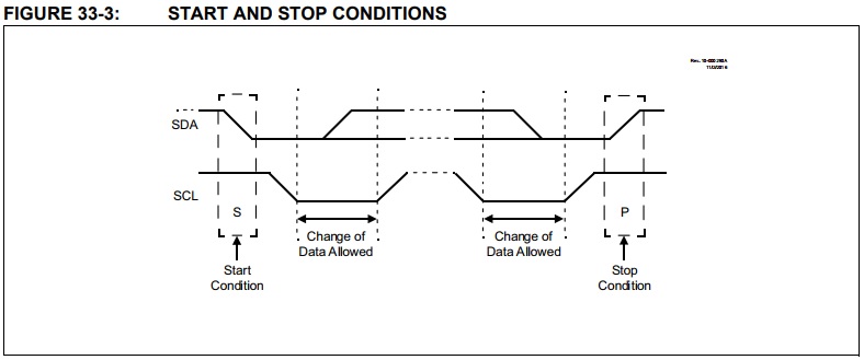
| 33.3.5 START ÁLLAPOT Az I2C specifikáció szerint a Start állapotot az, amikor az SDA vonal átmegy magas szintről alacsony szintre míg az SCL vonal magas szinten van. A Start jel mindig a master által generálódik, és a busz átállását pihenő állípotból aktív állapotba helyezi. A 33-3 ábra mutatja a kezdeti feltételekhez tartozó hullámformákat. A mester várja az I2CxSTAT0 BFRE bitjének beállítását, mielőtt az SCL és SDA vonalakra Start állapotot kiadja. Ha két mester egyszerre indítja el a startot, ütközés következik be a címzési fázis során. |
33.3.5 START CONDITION The I2C specification defines a Start condition as a transition of SDA line from a high to a low state while SCL line is high. A Start condition is always generated by the master and signifies the transition of the bus from an Idle to an Active state. Figure 33-3 shows waveforms for Start conditions. Master hardware waits for the BFRE bit of I2CxSTAT0 to be set, before asserting a Start condition on the SCL and SDA lines. If two masters assert a start at the same time, a collision will occur during the addressing phase. |
||||||||||||||||||||||||||||||||||||||||||||||||||||||||||||||||||||
| 33.3.6 STOP ÁLLAPOT A Stop állapot az SDA vonal átmenete alacsonyról magasra, míg az SCL vonal magas szinten van. A 33-3. Ábra a Stop állapotokra vonatkozó hullámalakokat mutatja. |
33.3.6 STOP CONDITION A Stop condition is a transition of the SDA line from low to high while the SCL line is high. Figure 33-3 shows waveforms for Stop conditions. |
||||||||||||||||||||||||||||||||||||||||||||||||||||||||||||||||||||
 |
|||||||||||||||||||||||||||||||||||||||||||||||||||||||||||||||||||||
| Megjegyzés: ??Legalább egy SCL alacsony időnek kell megjelennie, mielőtt a Stop érvényes. Ezért ha az SDA vonal alacsony, akkor ismét magas, ha az SCL vonal magas, akkor csak a Start állapot észlelhető.?? |
Note: At least one SCL low time must appear before a Stop is valid. Therefore if the SDA line goes low then high again whilthe SCL line is high, only the Start condition is detected. |
||||||||||||||||||||||||||||||||||||||||||||||||||||||||||||||||||||
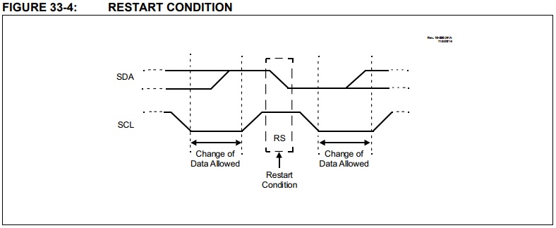
| 33.3.7 RESTART ÁLLAPOT A Restart minden olyan időpontban érvényes, amikor a Stop lesz érvényben. A mester kiadhat egy újraindítást, ha a buszot az aktuális átvitel befejezése után szeretné tartani. A Restart ugyanazt a hatást gyakorolja a slave-re, mint a Start, minden slave logikát visszaállítaná, és egy címre felkészítené. A mester érdemes ugyanazt vagy egy másik rabszolgát kezelni. A 33-4. Ábra mutatja az Újraindítás állapotának hullámformáját. 10 bites címzési slave üzemmódban újraindításra van szükség ahhoz, hogy a master a címzett slave-ből adatokat tárjon ki. Miután egy slave teljesen meg volt oldva, mind a magas, mind az alacsony cím bájtokkal (SMA = 1) egyezik meg, a master kiadhatja az újraindítást és a nagy cím bájtot az R / W bit készletével. A slave logika ezután megtartja az órát, és készen áll az adatok időzítésére. |
33.3.7 RESTART CONDITION A Restart is valid any time that a Stop would be valid. A master can issue a Restart if it wishes to hold the bus after terminating the current transfer. A Restart has the same effect on the slave that a Start would, resetting all slave logic and preparing it to clock in an address. The master may want to address the same or another slave. Figure 33-4 shows the waveform for a Restart condition. In 10-bit Addressing Slave mode a Restart is required for the master to clock data out of the addressed slave. Once a slave has been fully addressed, matching both high and low address bytes (SMA = 1), the master can issue a Restart and the high address byte with the R/W bit set. The slave logic will then hold the clock and prepare to clock out data. |
||||||||||||||||||||||||||||||||||||||||||||||||||||||||||||||||||||
 |
|||||||||||||||||||||||||||||||||||||||||||||||||||||||||||||||||||||
| 33.3.8 A MŰKÖDÉS IDŐRENDBENI LEFOLYÁSA A kilencedik SCL impulzuskor (szinkronjelkor) az adattvonalon (SDA) Az I2C-ben az elfogadás jelzésére szolgál a fogadó számára. Ez úgy valósuk meg, hogy a vevő az adatvonalat (SDA) alacsony szintre húzza. Természetesen az adónak erre az időre szabadon kell hagyni az adatvonalat és közben figyelni, hogy a vevő lehúzta-e az adatvonalat a szinkronjel magas értéke idelén. Tehát ez nem él, hanem jel lesz. Mindezt a vevő által küldött nyugtázásnak tekintjük, és ezt a jelet, pedig ACK jelnek hívjuk. Az ACK eredményét az I2CxCON1 regiszter ACKSTAT bitjébe helyezzük. A küldő 2CxCON1 regiszterének ACKSTAT bitje törlődik, amikor a fogadó készülék egy nyugtázást küld, és akkor lesz 1 az értéke, ha a fogadó készülék nem ismeri fel az adatot. Tehát mégegyszer tészletesebben: a szolga egy nyugtázást küld, amikor felismerte a címét. Ha az adatot fogadó üzemmódban az adókra küldött ACK adatok az I2CxCNT regiszter értékétől függenek. Az ACKDT az I2CxCNT értékkel küldött érték! = 0. Ha I2CxCNT = 0, akkor az ACKCNT értéket kell használni. Lave üzemmódban, ha az ADRIE vagy WRIE bitek be vannak állítva, az óraperiódás akkor kezdődik, ha van egy címegyeztetés, vagy amikor megpróbál írni a slave-nek. Ez lehetővé teszi a ser számára, hogy az ACK értéket visszaadja az adónak. Az I2CxCON1 regiszter ACKDT bitje be van állítva / törölve a válasz meghatározásához. A slave hardver generál egy ACK választ, ha az ADRIE vagy WRIE bitek világosak. Bizonyos feltételek miatt nem ACK (NACK) küldhető automatikusan. Ha az RXRE, TXRE, RXO vagy TXU bitek bármelyike be van állítva, akkor a hardveres válasz NACK-ra kényszerül. Minden eszközre adott válasz, amely a cím megegyezik vagy adatokkal történik, NACK válasz lesz. ELISMERNI |
33.3.8 ACKNOWLEDGE SEQUENCE The ninth SCL pulse for any transferred byte in I2C is dedicated as an Acknowledge. It allows receiving devices to respond back to the transmitter by pulling the SDA line low. The transmitter must release control of the line during this time to shift in the response. The Acknowledge (ACK) is an active-low signal, pulling the SDA line low indicates to the transmitter that the device has received the transmitted data and is ready to receive more. The result of an ACK is placed in the ACKSTAT bit of the I2CxCON1 register. The ACKSTAT bit is cleared when the receiving device sends an Acknowledge and is set when the receiving device does not Acknowledge. A slave sends an Acknowledge when it has recognized its address. When in a mode that is receiving data, the ACK data being sent to the transmitter depends on the value of I2CxCNT register. ACKDT is the value sent when I2CxCNT! = 0. When I2CxCNT = 0, the ACKCNT value is used instead. In lave mode, if the ADRIE or WRIE bits are set, clock stretching is initiated when there is an address match or when there is an attempt to write to slave. This allows the ser to set the ACK value sent back to the transmitter. The ACKDT bit of the I2CxCON1 register is set/cleared to determine the response. Slave hardware will generate an ACK response if the ADRIE or WRIE bits are clear. Certain conditions will cause a not-ACK (NACK) to be sent automatically. If any of the RXRE, TXRE, RXO, or TXU bits is set, the hardware response is forced to NACK. All subsequent responses from the device for address matches or data will be a NACK response. |
||||||||||||||||||||||||||||||||||||||||||||||||||||||||||||||||||||
| 33.3.9 BUS TIME-OUT The I2CxBTO register can be used to select the timeout source for the module. The I2C module is reset when the selected bus time out signal goes high. This feature is useful for SMBus and PMBus™ compatibility. For example, Timer2 can be selected as the bus timeout source and configured to count when the SCL pin is low. If the timer runs over before the SCL pin transitioned high, the timer-out pulse will reset the module. Note: The bus time-out source should produce arising edge. If the module is configured as a slave and a BTO event occurs when the slave is active, i.e., the SMA bit is set, the module is immediately reset. The SMA and CSTR bits are also cleared, and the BTOIF bit is set. If a BTO event occurs when the module is configured as a master and is active, (i.e., MMA bit is set), and the module immediately tries to assert a Stop condition and also sets the BTOIF bit. The actual generation of the Stop condition may be delayed if the bus is been clock stretched by some slave device. The MMA bit will be cleared only after the Stop condition is generated. If a BTO event occurs when the module is configured as a master and is active, (i.e., MMA bit is set), and the module immediately tries to assert a Stop condition and also sets the BTOIF bit. The actual generation of the Stop condition may be delayed if the bus is been clock stretched by some slave device. The MMA bit will be cleared only after the Stop condition is generated. |
|||||||||||||||||||||||||||||||||||||||||||||||||||||||||||||||||||||
| 33.3.10 ADDRESS BUFFERS The I2C module has two address buffer registers, I2CxADB0 and I2CxADB1. Depending on the mode, these registers are used as either receive or transmit address buffers. See Table 33-2 for data flow directions in these registers. In Slave modes, these registers are only updated when there is an address match. The ADB bit in the I2CxCON2 register is used to enable/disable the address buffer functionality. When disabled, the address data is sourced from the transmit buffer and is stored in the receive buffer. |
|||||||||||||||||||||||||||||||||||||||||||||||||||||||||||||||||||||
|
|||||||||||||||||||||||||||||||||||||||||||||||||||||||||||||||||||||
| 33.3.10.1 Slave Mode (7-bit) In 7-bit Slave mode, I2CxADB0 is loaded with the received matching address and R/W data. The I2CxADB1 register is ignored in this mode. |
|||||||||||||||||||||||||||||||||||||||||||||||||||||||||||||||||||||
| 33.3.10.2 Slave Mode (10-bit) In 10-bit Slave mode, I2CxADB0 is loaded with the lower eight bits of the matching received address. I2CxADB1 is loaded with full eight bits of the high address byte, including the R/W bit. |
|||||||||||||||||||||||||||||||||||||||||||||||||||||||||||||||||||||
| 33.3.10.3 Master Mode (7-bit) The I2CxADB0 register is ignored in this mode. In 7-bit Master mode, the I2CxADB1 register is used to copy address data byte, including the R/W value, to the shift register. |
|||||||||||||||||||||||||||||||||||||||||||||||||||||||||||||||||||||
| 33.3.10.4 Master Mode (10-bit) In 10-bit Master mode, the I2CxADB0 register stores the low address data byte value that will be copied to the shift register after the high address byte is shifted out. The I2CxADB1 register stores the high address byte value that will be copied to the shift register. It is up to the user to specify all ei ght of these bits, even though the I2C specification defines the upper five bits as a constant. |
|||||||||||||||||||||||||||||||||||||||||||||||||||||||||||||||||||||
| 33.3.10.5 Multi-Master Mode (7-bit only) In Multi-Master mode, the device can be both master and slave depending on the sequence of events on the bus. If being addressed as a slave, the I2CxADB0 register stores the received matching slave address byte. If the device is trying to communicate as a master on the bus, the contents of the I2CxADB1 register are copied to the shift register for addressing a slave device. |
|||||||||||||||||||||||||||||||||||||||||||||||||||||||||||||||||||||
| 33.3.11 RECEIVE AND TRANSMIT BUFFER The receive buffer holds one byte of data while another is shifted into the SDA pin. The user can access the buffer by software (or DMA) through the I2CxRXB register. When new data is loaded into the I2CxRXB register, the receive buffer full Status bit (RXBF) is set and reading the I2CxRXB register clears this bit. If the user tries to read I2CxRXB when it is empty (i.e., RXBF = 0), receive read error bit (RXRE) is set and a NACK will be generated. The user must clear the error bit to resume normal operation. The ransmit buffer holds one byte of data while another can be shifted out through the SDA pin. The user can access the buffer by software (or DMA) through the I2CxTXB register. When the I2CxTXB does not contain any transmit data, the transmit buffer empty status bit (TXBE) is set. At this point, the user can load another byte into the buffer. If the user tries to write I2CxTXB when it is NOT empty (i.e. TXBE = 0), transmit write error flag bit (TXRE) is set and the new data is discarded. When TXRE is et, the user must clear this error condition to resume normal operation. By setting the CLRBF bit in the I2CxSTAT1 register, the user can clear both receive and transmit buffers. CLRBF will also clear the I2CxRXIF and I2CxTXIF bits. |
|||||||||||||||||||||||||||||||||||||||||||||||||||||||||||||||||||||
| 33.3.12 CLOCK STRETCHING When a slave device has not completed processing data, it can delay the transfer of more data through the process of clock stretching. An addressed slave device may hold the SCL clock line low after receiving or sending a bit, indicating that it is not yet ready to continue. The master will attempt to raise the SCL line in order to transfer the next bit, but will detect that the clock line has not yet been released. Since the SCL connection is open-drain, the slave has the ability to hold the line low until it is ready to continue communicating. Clock stretching allows receivers that cannot keep up with a transmitter to control the flow of incoming data. Clock stretching can be enabled or disabled by the clearing or setting of CSTRDIS (clock stretching disable) bit in the I2CxCON2 register. This bit is valid only in the Multi-Master and Slave modes of operation. |
|||||||||||||||||||||||||||||||||||||||||||||||||||||||||||||||||||||
| 33.3.12.1 Clock Stretching for Buffer Operations If enabled, clock stretching is forced during buffer read/write operations. For example, in Slave mode if RXBF = 1 (receive buffer full), the clock will be stretched after the seventh falling edge of SCL. The SCL line is released only after the user reads data from the receive buffer. This ensures that there is never a receive data overflow. In this situation, if clock stretching is disabled, the RXO bit in I2CxCON1 is set indicating a receive overflow. When set, the module will always respond with a NACK. Similarly, when TXBE = 1 (transmit buffer empty) and I2CCNT! = 0, the clock is stretched after the 8th falling edge of SCL. The SCL line is released only after the user loads new data into the transmit buffer. This ensures that there is never a transmit underflow. In this situation, if clock stretching is disabled, the TXUF bit in I2CxCON1 is set indicating a transmit underflow. When set, the module will always respond with a NACK. |
|||||||||||||||||||||||||||||||||||||||||||||||||||||||||||||||||||||
| 33.3.12.2 Clock Stretching for Other Slave Operations There are three Interrupt and Hold bits that provide clock stretching in Slave mode. These bits can also be used in conjunction with the I2CxIE bit in PIRx register to generate system level interrupts. • Incoming address match interrupt - Clock stretching after an incoming matching address byte is enabled by the Address Interrupt and Hold (ADRIE) bit of the I2CxPIE register. When ADRIE = 1, the CSTR bit is set and the SCL line is stretched following the 8th falling edge of SCL of a received matching address. This allows the user to read the received address from the I2CADB0/1 registers and selectively ACK/NACK based on the received address. Clock stretching from ADRIE is released by software clearing the CSTR bit. • Data Write Interrupt - The data write interrupt and hold enable (WRIE) bit is used to enable clock stretching after a received data byte. When WRIE = 1, the CSTR bit is set, and the SCL line is stretched, following the 8th falling SCL edge for incoming slave data. This bit allows user software to selectiv ely ACK/NACK each received data byte. Clock stretching from WRIE is released by software clearing the CSTR bit. • Acknowledge status - The acknowledge status time interrupt and hold enable (ACKTIE) bit is used to enable clock stretching after the ACK phase of a transmission. This bit enables clock stretching for all address/data transactions; address, write, or read. Following the ACK, the slave hardware will set CSTR. Clock stretching from ACKTIE is released by software clearing the CSTR bit. |
|||||||||||||||||||||||||||||||||||||||||||||||||||||||||||||||||||||
| 33.3.13 DATA BYTE COUNT The I2CxCNT register is used to specify the number of bytes in a complete I2C packet. The value in this register will decrement every time a data byte is received or transmitted from the I2C module. The I2CxCNT register will not decrement past zero. If a byte transfer causes the I2CxCNT register to decrement to zero, the Count Interrupt Flag bit (CNTIF) in I2CxPIR is set. This flag bit is set on the 9 th falling edge of SCL for transmit operations and can be more informational if the edge is specified. The I2CxCNT register can be auto-loaded if the ACNT bit in the I2CxCON2 register is set. When ACNT bit is set, the data byte following the address byte is loadedinto the I2CxCNT register. |
|||||||||||||||||||||||||||||||||||||||||||||||||||||||||||||||||||||
|
Note:
|
|||||||||||||||||||||||||||||||||||||||||||||||||||||||||||||||||||||
| 3.4 I2C Slave Mode The I2C Slave mode operates in one of four modes selected in the Mode bits of I2CxCON0. The modes can be divided into 7- and 10-bit Addressing modes. 10-bit Addressing modes operate the same as 7-bit with some additional overhead for handling the larger addresses. |
|||||||||||||||||||||||||||||||||||||||||||||||||||||||||||||||||||||
| 33.4.1 SLAVE ADDRESSING MODES The I2CxADR/1/2/3 registers contain the Slave mode addresses. The first byte received after a Start or Restart condition is compared against the values stored in these registers. If the byte matches a value, it is loaded into the I2CxADB0/1 registers. If the value does not match, there is no response from the module. The I2C module can be configured in the following Slave configurations. |
|||||||||||||||||||||||||||||||||||||||||||||||||||||||||||||||||||||
| 33.4.1.1 7-bit Addresses Mode In this mode, the LSb of the received data byte is ignored when determining if there is an address match. All four I2CxADR registers are independently compared to the received address byte. |
|||||||||||||||||||||||||||||||||||||||||||||||||||||||||||||||||||||
| 33.4.1.2 7-bit Addresses with Masking In this mode, the value in I2CxADR0 is masked with the value in I2CxADR1 to determine if an address match occurred. A second address and mask are also compared from I2CxADR2/3. When Mode<2:0> = 001 or 111, the I2CxADR1/3 registers serve as the mask value for I2CxADR0/2. All seven bits of the address can be masked |
|||||||||||||||||||||||||||||||||||||||||||||||||||||||||||||||||||||
| 33.4.1.3 10-bit Addresses In this mode, the values stored in I2CxADR0 and I2CxADR1 registers are used to create a 10-bit address. A second 10-bit compare address is formed from I2CxADR2 and I2CxADR3. |
|||||||||||||||||||||||||||||||||||||||||||||||||||||||||||||||||||||
| 33.4.1.4 10-bit Address with Masking In this mode, the I2CxADR0/1 registers are used to form a 10-bit address, and the I2CxADR2/3 registers are used to form a 10-bit mask for that address. When MODE<2:0> = 011, the I2CxADR2/3 registers serve as the mask value for the 10-bit address stored in I2CxADR0/1. |
|||||||||||||||||||||||||||||||||||||||||||||||||||||||||||||||||||||
| Note: Even though 10-bit addressing calls out only 10-bits used in the address comparison, all 15 address bits in I2CxADR0/1 are compared in these modes. |
|||||||||||||||||||||||||||||||||||||||||||||||||||||||||||||||||||||
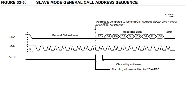
| 33.4.2 GENERAL CALL ADDRESS SUPPORT The addressing procedure for the I2C bus is such that the first byte after the Start condition usually determines which device will be the slave addressed by the master device. The exc eption is the general call address which can address all devices. When this address is used, all devices should, in theory, respond with an ACK. The general call address is a reserved address in the I2C protocol, defined as address 0x00. In order for the slave hardware to ACK this address, it must be enabled by setting the GCEN bit in the I2CxCON2 register. Setting one of the I2CxADR0/1/2/3 registers to 0x00 is not required. Figure 33-5 shows a General Call reception sequence. If the ADRIE bit is set, the module will clock stretch after the eighth SCL pulse just like any other address match. |
|||||||||||||||||||||||||||||||||||||||||||||||||||||||||||||||||||||
| Note: General Call addressing is supported in only 7-bit Addressing modes |
|||||||||||||||||||||||||||||||||||||||||||||||||||||||||||||||||||||
 |
|||||||||||||||||||||||||||||||||||||||||||||||||||||||||||||||||||||
| 33.4.3 SLAVE OPERATION IN 7-BIT ADDRESSING MODE The 8th bit in an address byte transmitted by the master is used to determine if the Master wants to read from or write to the Slave device. If set, it denotes that the Master wants to read from the slave and if cleared it means the master wants to write to the slave device. If there is an address match, the R/W bit is copied to the R/W bit of the I2CxSTAT0 register. |
|||||||||||||||||||||||||||||||||||||||||||||||||||||||||||||||||||||
| -------------------------------------------- | |||||||||||||||||||||||||||||||||||||||||||||||||||||||||||||||||||||