- Címlap
- LED kijelzők meghajtása
- Permetező projekt
- PIC18FxxK42
- PIC18FxxK42 I2C regiszterei
- PIC18FxxK42 órajel beállítása
- Pic18FxxK42 regiszterei
- Láb hozzárendelés PIC18FxxK42
- Pic18 I2C programozás
- PIC18FxxK42 I2C kommunikáció
- EEPROM memória használata
- LIN UART-tal fordítás
- LM75A és PIC18F45K42 I2C1 program
- Objektumok
- Pic18FxxK42 konfigurálás
- SPI
- UART PIC18(L)F45K42
- Watchdog Timer
- PIC18F45K42 timer2,-4,-6
- I2C modul 1
- PIC18F45K22 I2C lépései
- PIC18F45K42 USART regiszterei és azok magyarázata II.
- PIC18F45K42 USART regiszterei
- PIC18F45K42 timer1,-3,-5
- UART PIC18F45K42
- PIC18 utasításkészlete
- USART mudullal aszinkron kapcsolat két mikrokontroller közt
- CAN kommunikáció
- DS3231SN RTC
- Dell T 5600
- E-paper
- EGYÉB jegyzet
- ESP 8266 WiFi modul
- ESP-07 ESP-12x
- ESP-12F WiFi modul
- ESP32
- ESP8266
- Egyéb (elektronika)
- Emeléskijelző projekt
- Giroszkóp
- HASZNOSAK
- Hasznos általános linkek
- Illesztő modulok
- Kapcsolások, megoldások
- Kiszajú műveleti erősítő
- Konfigurálás
- LIN kommunikáció UART-tal
- MPASM PIC18
- Nyomásmérés MS5803-05BA-val
- Nyomásmérő I2C
- Nyomásszenzor SPD8xx I2C
- Nyák, nyáktervezés
- Operációs rendszerek
- PIC 18 mikrokontrollerek
- PIC18(L)F47K40
- PIC18(L)F65K40
- PIC18F45(K)50
- PIC18F87k22(80 láb)
- PROGRAMOZÁS
- Programozás
- Python 3
- RAUCH 2057153
- RDS
- RTC TLC 5947-el
- Rádiókapcsolat két mikrokontroller között
- Számítógépes programok
- TCS34725 színérzékelő
- TLC 5947
- TTP223 kapacitív nyomógomb
- USB + USB AN1310-el
- Ulefone Power 2
- Vektoros megszakítások
- Vetőgép
- Webfejlesztés
- WiFi, Bluetooth modulok
- Pickit 3 programozó
- Pic-Ethernet-Pic
- LM75A
- PWM CCPx modullal
- PWM PWMx modullal
- NCO
- TCS 3200 RGB érzékelés
- Nyáktervezés
- Oktatás
- PIC 24 mikrokontrollerek
Érdeklődési kör: elektronika, programozás, mikrokontroller programozás
PIC18FxxK42
Új adatlap: http://ww1.microchip.com/downloads/en/DeviceDoc/PIC18LF26-27-45-46-47-55-56-57K42-Data-Sheet-40001919E.pdf
Programozási megoldás "case" esetén PCL, (PCH, PCU) és PCLATH, PCLATU felhasználásával : http://www.t-es-t.hu/elokep/pic/felhkk/kk/sz100101.htm (Ezt áttenni asm kategóriába!)
Online baudrata genetátor: http://www.nicksoft.info/el/calc/?ac=spbrg
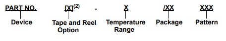
| Device: | Pld.: PIC18(L)FxxK42-nál: PIC18F26K42, PIC18LF26K42, PIC18F27K42, PIC18LF27K42, IC18F45K42, PIC18LF45K42, PIC18F46K42, PIC18LF46K42, PIC18F47K42, PIC18LF47K42, PIC18F55K42, PIC18LF55K42, PIC18F56K42, PIC18LF56K42, PIC18F57K42, PIC18LF57K42 |
| Tape and Reel Option: | Blank = standard packaging (tube or tray) T = Tape and Reel(1), (2) |
| Temperature Range: |
E= -40°C to +125°C (Extended) I= -40°C to +85°C (Industrial) |
| Package: | ML = 28-lead QFN 6x6mm ML = 44-lead QFN 8x8x0.9mm MX = 28-lead UQFN 6x6x0.5mm MV = 40-lead UQFN 5x5x0.5mm MV = 48-lead UQFN P = 40-lead PDIP PT = 44-lead TQFP (Thin Quad Flatpack) PT = 48-lead TQFP SO = 28-lead SOIC SP = 28-lead Skinny Plastic DIP SS = 28-lead SSOP |
| Pattern: | QTP, SQTP, Code or Special Requirements (blank otherwise) |
Note 1:
Tape and Reel option is available for ML, MV, PT, SO and SS packages with industrial Temperature Range only.
Note 2:
Tape and Reel identifier only appears in catalog part number description. This identifier is used for ordering purposes and is not printed on the device package.
;konfigurációs bitek
; A CONFIG direktívával lehet megadni a konfiguráci
ó adatait.
; A szimbólumok azonosak a P18F442.INC fájlban mega
dottakkal.
; The PIC18FXX2 adatlapja tartalmazza konfigurációs
bitek leírását.
; A következ
ı
sorokat az alkalmazáshoz illeszked
ı
en meg kell változtatni.
;CONFIG OSC=XT
;kvarc oszcillátor
CONFIG OSC=INTIO67
;bels
ı
kvarc oszcillátor RA6-7 láb üzemel
CONFIG FCMEN=ON
;oszcillátor monitorozás be
CONFIG IESO=OFF
;bels
ı
-küls
ı
oszcillátor váltás ki
CONFIG PWRT=ON
;oszcillátor bekapcsolása akkor, ha
stabil a táp
CONFIG BOREN=ON
;kritikus tápfeszültség reszet be
CONFIG BORV=2
;reszet szintje
CONFIG WDT=ON
;watchdog timer be
CONFIG WDTPS=128
;128-as el
ı
osztó
CONFIG MCLRE=OFF
;reszet láb ki, MCLR I/O lábként
üzemel
CONFIG LPT1OSC=OFF ;másodlagos oszcillátor ki
CONFIG PBADEN=OFF ;PORTB0-4 digitális I/O
CONFIG STVREN=OFF
;reszet verem túl-alul csordulá
s hatására ki
CONFIG LVP=OFF
;alacsony feszültség
ő
programozás ki
CONFIG XINST=OFF
;kiterjesztett utasításkészlet ki
, indexelés ki
CONFIG DEBUG=OFF
;nyomkövetés ki
CONFIG CP0=OFF
;kódvédelem ki
CONFIG CP1=OFF
CONFIG CPB=ON
;boot-blokk védelem (1. 128 sor) be
CONFIG CPD=OFF
;EEPROM védelem ki
CONFIG WRT0=OFF
;programmemória írásvédelem ki
CONFIG WRT1=OFF
CONFIG WRTB=OFF
;tábla írásvédelem ki
CONFIG WRTC=OFF
;konfigurációs bitek írásvédelme k
i
CONFIG WRTD=OFF
;EEPROM írásvédelme ki
CONFIG EBTR0=OFF
;tábla kiolvasás védelem ki
CONFIG EBTR1=OFF
CONFIG EBTRB=OFF
Alkalmazott mikroprocesszor (leírás): PIC18F45K42
Adatlap (pdf): PIC18F(L)xxK42.pdf
PIC18F45K42
Láb összerendelések (honlapomon): http://www.kovacsistvan.kkfh.hu/node/26
Regiszter összesítő és elérése (honlapomon): itt
Vektoros megszakításokról leírás (nem pont erre a típusra): http://esca.atomki.hu/PIC24/interrupts.html
I2C lábak összerendelése (megj.: 2 db I2C van egy tokban megvalósítva) :
I2C1 Clock (órajel) alapértelmezésben az RC3-hoz van rendelve, módosítható az I2C1SCLPPS regiszterrrel.
I2C1 Data (adat láb) alapértelmezésben az RC4-hez van rendelve, módosítható az I2C1SDAPPS regiszterrel.
A kivezetések módosítása csak az A és/vagy C porton belül lehet.
I2C2 Clock (órajel) alapértelmezésben az RB1-hoz van rendelve, módosítható az I2C2SCLPPS regiszterrrel.
I2C2 Data (adat láb) alapértelmezésben az RB2-hez van rendelve, módosítható az I2C2SDAPPS regiszterrel.
A kivezetések módosítása csak a B és/vagy D porton belül lehet.
Ezek az adatlap 279-es oldalán szerepelnek.
A megszakítás regiszterek a 169-es oldalon szerepelnek.
A ládhozzárendelő PPS regiszterek a 272-tól, de a 277 oldalon vannak.
A használt regiszterek listája az 595-ös oldalon találhatók.
Kimeneti lábak a 280. oldalon
I2C1 Clock
RC3
Konfigurálás:
;
; IMPORTANT: For the PIC18 devices, the __CONFIG directive has been
; superseded by the CONFIG directive. The following settings
; are available for this device.
;
; External Oscillator Selection:
; FEXTOSC = LP LP (crystal oscillator) optimized for 32.768 kHz; PFM set to low power
; FEXTOSC = XT XT (crystal oscillator) above 100 kHz, below 8 MHz; PFM set to medium power
; FEXTOSC = HS HS (crystal oscillator) above 8 MHz; PFM set to high power
; FEXTOSC = RESERVED Reserved (DO NOT USE)
; FEXTOSC = OFF Oscillator not enabled
; FEXTOSC = ECL EC (external clock) below 100 kHz; PFM set to low power
; FEXTOSC = ECM EC (external clock) for 500 kHz to 8 MHz; PFM set to medium power
; FEXTOSC = ECH EC (external clock) above 8 MHz; PFM set to high power
;
; Reset Oscillator Selection:
; RSTOSC = HFINTOSC_64MHZHFINTOSC with HFFRQ = 64 MHz and CDIV = 1:1
; RSTOSC = RESERVED_1 Reserved
; RSTOSC = EXTOSC_4PLL EXTOSC with 4x PLL, with EXTOSC operating per FEXTOSC bits
; RSTOSC = RESERVED_2 Reserved
; RSTOSC = SOSC Secondary Oscillator
; RSTOSC = LFINTOSC Low-Frequency Oscillator
; RSTOSC = HFINTOSC_1MHZHFINTOSC with HFFRQ = 4 MHz and CDIV = 4:1
; RSTOSC = EXTOSC EXTOSC operating per FEXTOSC bits (device manufacturing default)
;
; Clock out Enable bit:
; CLKOUTEN = ON CLKOUT function is enabled
; CLKOUTEN = OFF CLKOUT function is disabled
;
; PRLOCKED One-Way Set Enable bit:
; PR1WAY = OFF PRLOCK bit can be set and cleared repeatedly
; PR1WAY = ON PRLOCK bit can be cleared and set only once
;
; Clock Switch Enable bit:
; CSWEN = OFF The NOSC and NDIV bits cannot be changed by user software
; CSWEN = ON Writing to NOSC and NDIV is allowed
;
; Fail-Safe Clock Monitor Enable bit:
; FCMEN = OFF Fail-Safe Clock Monitor disabled
; FCMEN = ON Fail-Safe Clock Monitor enabled
;
; MCLR Enable bit:
; MCLRE = INTMCLR If LVP = 0, MCLR pin function is port defined function; If LVP =1, RE3 pin fuction is MCLR
; MCLRE = EXTMCLR If LVP = 0, MCLR pin is MCLR; If LVP = 1, RE3 pin function is MCLR
;
; Power-up timer selection bits:
; PWRTS = PWRT_1 PWRT set at 1ms
; PWRTS = PWRT_16 PWRT set at 16ms
; PWRTS = PWRT_64 PWRT set at 64ms
; PWRTS = PWRT_OFF PWRT is disabled
;
; Multi-vector enable bit:
; MVECEN = OFF Interrupt contoller does not use vector table to prioritze interrupts
; MVECEN = ON Multi-vector enabled, Vector table used for interrupts
;
; IVTLOCK bit One-way set enable bit:
; IVT1WAY = OFF IVTLOCK bit can be cleared and set repeatedly
; IVT1WAY = ON IVTLOCK bit can be cleared and set only once
;
; Low Power BOR Enable bit:
; LPBOREN = ON ULPBOR enabled
; LPBOREN = OFF ULPBOR disabled
;
; Brown-out Reset Enable bits:
; BOREN = OFF Brown-out Reset disabled
; BOREN = ON Brown-out Reset enabled according to SBOREN
; BOREN = NOSLP Brown-out Reset enabled while running, disabled in Sleep; SBOREN is ignored
; BOREN = SBORDIS Brown-out Reset enabled , SBOREN bit is ignored
;
; Brown-out Reset Voltage Selection bits:
; BORV = VBOR_2P85 Brown-out Reset Voltage (VBOR) set to 2.8V
; BORV = VBOR_2P7 Brown-out Reset Voltage (VBOR) set to 2.7V
; BORV = VBOR_245 Brown-out Reset Voltage (VBOR) set to 2.45V
; BORV = VBOR_2P45 Brown-out Reset Voltage (VBOR) set to 2.45V
;
; ZCD Disable bit:
; ZCD = ON ZCD always enabled
; ZCD = OFF ZCD disabled. ZCD can be enabled by setting the ZCDSEN bit of ZCDCON
;
; PPSLOCK bit One-Way Set Enable bit:
; PPS1WAY = OFF PPSLOCK bit can be set and cleared repeatedly (subject to the unlock sequence)
; PPS1WAY = ON PPSLOCK bit can be cleared and set only once; PPS registers remain locked after one clear/set cycle
;
; Stack Full/Underflow Reset Enable bit:
; STVREN = OFF Stack full/underflow will not cause Reset
; STVREN = ON Stack full/underflow will cause Reset
;
; Debugger Enable bit:
; DEBUG = ON Background debugger enabled
; DEBUG = OFF Background debugger disabled
;
; Extended Instruction Set Enable bit:
; XINST = ON Extended Instruction Set and Indexed Addressing Mode enabled
; XINST = OFF Extended Instruction Set and Indexed Addressing Mode disabled
;
; WDT Period selection bits:
; WDTCPS = WDTCPS_0 Divider ratio 1:32
; WDTCPS = WDTCPS_1 Divider ratio 1:64
; WDTCPS = WDTCPS_2 Divider ratio 1:128
; WDTCPS = WDTCPS_3 Divider ratio 1:256
; WDTCPS = WDTCPS_4 Divider ratio 1:512
; WDTCPS = WDTCPS_5 Divider ratio 1:1024
; WDTCPS = WDTCPS_6 Divider ratio 1:2048
; WDTCPS = WDTCPS_7 Divider ratio 1:4096
; WDTCPS = WDTCPS_8 Divider ratio 1:8192
; WDTCPS = WDTCPS_9 Divider ratio 1:16384
; WDTCPS = WDTCPS_10 Divider ratio 1:32768
; WDTCPS = WDTCPS_11 Divider ratio 1:65536
; WDTCPS = WDTCPS_12 Divider ratio 1:131072
; WDTCPS = WDTCPS_13 Divider ratio 1:262144
; WDTCPS = WDTCPS_14 Divider ratio 1:524299
; WDTCPS = WDTCPS_15 Divider ratio 1:1048576
; WDTCPS = WDTCPS_16 Divider ratio 1:2097152
; WDTCPS = WDTCPS_17 Divider ratio 1:4194304
; WDTCPS = WDTCPS_18 Divider ratio 1:8388608
; WDTCPS = WDTCPS_19 Divider ratio 1:32
; WDTCPS = WDTCPS_20 Divider ratio 1:32
; WDTCPS = WDTCPS_21 Divider ratio 1:32
; WDTCPS = WDTCPS_22 Divider ratio 1:32
; WDTCPS = WDTCPS_23 Divider ratio 1:32
; WDTCPS = WDTCPS_24 Divider ratio 1:32
; WDTCPS = WDTCPS_25 Divider ratio 1:32
; WDTCPS = WDTCPS_26 Divider ratio 1:32
; WDTCPS = WDTCPS_27 Divider ratio 1:32
; WDTCPS = WDTCPS_28 Divider ratio 1:32
; WDTCPS = WDTCPS_29 Divider ratio 1:32
; WDTCPS = WDTCPS_30 Divider ratio 1:32
; WDTCPS = WDTCPS_31 Divider ratio 1:65536; software control of WDTPS
;
; WDT operating mode:
; WDTE = OFF WDT Disabled; SWDTEN is ignored
; WDTE = SWDTEN WDT enabled/disabled by SWDTEN bit
; WDTE = NSLEEP WDT enabled while sleep=0, suspended when sleep=1; SWDTEN ignored
; WDTE = ON WDT enabled regardless of sleep
;
; WDT Window Select bits:
; WDTCWS = WDTCWS_0 window delay = 87.5; no software control; keyed access required
; WDTCWS = WDTCWS_1 window delay = 75 percent of time; no software control; keyed access required
; WDTCWS = WDTCWS_2 window delay = 62.5 percent of time; no software control; keyed access required
; WDTCWS = WDTCWS_3 window delay = 50 percent of time; no software control; keyed access required
; WDTCWS = WDTCWS_4 window delay = 37.5 percent of time; no software control; keyed access required
; WDTCWS = WDTCWS_5 window delay = 25 percent of time; no software control; keyed access required
; WDTCWS = WDTCWS_6 window always open (100%); no software control; keyed access required
; WDTCWS = WDTCWS_7 window always open (100%); software control; keyed access not required
;
; WDT input clock selector:
; WDTCCS = LFINTOSC WDT reference clock is the 31.0 kHz LFINTOSC
; WDTCCS = MFINTOSC WDT reference clock is the 32kHz MFINTOSC output
; WDTCCS = SOSC WDT reference clock is SOSC
; WDTCCS = SC Software Control
;
; Boot Block Size selection bits:
; BBSIZE = BBSIZE_8192 Boot Block size is 8192 words
; BBSIZE = BBSIZE_4096 Boot Block size is 4096 words
; BBSIZE = BBSIZE_2048 Boot Block size is 2048 words
; BBSIZE = BBSIZE_1024 Boot Block size is 1024 words
; BBSIZE = BBSIZE_512 Boot Block size is 512 words
;
; Boot Block enable bit:
; BBEN = ON Boot block enabled
; BBEN = OFF Boot block disabled
;
; Storage Area Flash enable bit:
; SAFEN = ON SAF enabled
; SAFEN = OFF SAF disabled
;
; Application Block write protection bit:
; WRTAPP = ON Application Block write protected
; WRTAPP = OFF Application Block not write protected
;
; Configuration Register Write Protection bit:
; WRTB = ON Configuration registers (300000-30000Bh) write-protected
; WRTB = OFF Configuration registers (300000-30000Bh) not write-protected
;
; Boot Block Write Protection bit:
; WRTC = ON Boot Block (000000-0007FFh) write-protected
; WRTC = OFF Boot Block (000000-0007FFh) not write-protected
;
; Data EEPROM Write Protection bit:
; WRTD = ON Data EEPROM write-protected
; WRTD = OFF Data EEPROM not write-protected
;
; SAF Write protection bit:
; WRTSAF = ON SAF Write Protected
; WRTSAF = OFF SAF not Write Protected
;
; Low Voltage Programming Enable bit:
; LVP = OFF HV on MCLR/VPP must be used for programming
; LVP = ON Low voltage programming enabled. MCLR/VPP pin function is MCLR. MCLRE configuration bit is ignored
;
; PFM and Data EEPROM Code Protection bit:
; CP = ON PFM and Data EEPROM code protection enabled
; CP = OFF PFM and Data EEPROM code protection disabled
;
;==========================================================================
;==========================================================================
;
; Configuration Bits
;
; NAME Address
; CONFIG1L 300000h
; CONFIG1H 300001h
; CONFIG2L 300002h
; CONFIG2H 300003h
; CONFIG3L 300004h
; CONFIG3H 300005h
; CONFIG4L 300006h
; CONFIG4H 300007h
; CONFIG5L 300008h
; CONFIG5H 300009h
;
;=================================
Amgol ereseti:
;
; IMPORTANT: For the PIC18 devices, the __CONFIG directive has been
; superseded by the CONFIG directive. The following settings
; are available for this device.
;
; External Oscillator Selection:
; FEXTOSC = LP LP (crystal oscillator) optimized for 32.768 kHz; PFM set to low power
; FEXTOSC = XT XT (crystal oscillator) above 100 kHz, below 8 MHz; PFM set to medium power
; FEXTOSC = HS HS (crystal oscillator) above 8 MHz; PFM set to high power
; FEXTOSC = RESERVED Reserved (DO NOT USE)
; FEXTOSC = OFF Oscillator not enabled
; FEXTOSC = ECL EC (external clock) below 100 kHz; PFM set to low power
; FEXTOSC = ECM EC (external clock) for 500 kHz to 8 MHz; PFM set to medium power
; FEXTOSC = ECH EC (external clock) above 8 MHz; PFM set to high power
;
; Reset Oscillator Selection:
; RSTOSC = HFINTOSC_64MHZHFINTOSC with HFFRQ = 64 MHz and CDIV = 1:1
; RSTOSC = RESERVED_1 Reserved
; RSTOSC = EXTOSC_4PLL EXTOSC with 4x PLL, with EXTOSC operating per FEXTOSC bits
; RSTOSC = RESERVED_2 Reserved
; RSTOSC = SOSC Secondary Oscillator
; RSTOSC = LFINTOSC Low-Frequency Oscillator
; RSTOSC = HFINTOSC_1MHZHFINTOSC with HFFRQ = 4 MHz and CDIV = 4:1
; RSTOSC = EXTOSC EXTOSC operating per FEXTOSC bits (device manufacturing default)
;
; Clock out Enable bit:
; CLKOUTEN = ON CLKOUT function is enabled
; CLKOUTEN = OFF CLKOUT function is disabled
;
; PRLOCKED One-Way Set Enable bit:
; PR1WAY = OFF PRLOCK bit can be set and cleared repeatedly
; PR1WAY = ON PRLOCK bit can be cleared and set only once
;
; Clock Switch Enable bit:
; CSWEN = OFF The NOSC and NDIV bits cannot be changed by user software
; CSWEN = ON Writing to NOSC and NDIV is allowed
;
; Fail-Safe Clock Monitor Enable bit:
; FCMEN = OFF Fail-Safe Clock Monitor disabled
; FCMEN = ON Fail-Safe Clock Monitor enabled
;
; MCLR Enable bit:
; MCLRE = INTMCLR If LVP = 0, MCLR pin function is port defined function; If LVP =1, RE3 pin fuction is MCLR
; MCLRE = EXTMCLR If LVP = 0, MCLR pin is MCLR; If LVP = 1, RE3 pin function is MCLR
;
; Power-up timer selection bits:
; PWRTS = PWRT_1 PWRT set at 1ms
; PWRTS = PWRT_16 PWRT set at 16ms
; PWRTS = PWRT_64 PWRT set at 64ms
; PWRTS = PWRT_OFF PWRT is disabled
;
; Multi-vector enable bit:
; MVECEN = OFF Interrupt contoller does not use vector table to prioritze interrupts
; MVECEN = ON Multi-vector enabled, Vector table used for interrupts
;
; IVTLOCK bit One-way set enable bit:
; IVT1WAY = OFF IVTLOCK bit can be cleared and set repeatedly
; IVT1WAY = ON IVTLOCK bit can be cleared and set only once
;
; Low Power BOR Enable bit:
; LPBOREN = ON ULPBOR enabled
; LPBOREN = OFF ULPBOR disabled
;
; Brown-out Reset Enable bits:
; BOREN = OFF Brown-out Reset disabled
; BOREN = ON Brown-out Reset enabled according to SBOREN
; BOREN = NOSLP Brown-out Reset enabled while running, disabled in Sleep; SBOREN is ignored
; BOREN = SBORDIS Brown-out Reset enabled , SBOREN bit is ignored
;
; Brown-out Reset Voltage Selection bits:
; BORV = VBOR_2P85 Brown-out Reset Voltage (VBOR) set to 2.8V
; BORV = VBOR_2P7 Brown-out Reset Voltage (VBOR) set to 2.7V
; BORV = VBOR_245 Brown-out Reset Voltage (VBOR) set to 2.45V
; BORV = VBOR_2P45 Brown-out Reset Voltage (VBOR) set to 2.45V
;
; ZCD Disable bit:
; ZCD = ON ZCD always enabled
; ZCD = OFF ZCD disabled. ZCD can be enabled by setting the ZCDSEN bit of ZCDCON
;
; PPSLOCK bit One-Way Set Enable bit:
; PPS1WAY = OFF PPSLOCK bit can be set and cleared repeatedly (subject to the unlock sequence)
; PPS1WAY = ON PPSLOCK bit can be cleared and set only once; PPS registers remain locked after one clear/set cycle
;
; Stack Full/Underflow Reset Enable bit:
; STVREN = OFF Stack full/underflow will not cause Reset
; STVREN = ON Stack full/underflow will cause Reset
;
; Debugger Enable bit:
; DEBUG = ON Background debugger enabled
; DEBUG = OFF Background debugger disabled
;
; Extended Instruction Set Enable bit:
; XINST = ON Extended Instruction Set and Indexed Addressing Mode enabled
; XINST = OFF Extended Instruction Set and Indexed Addressing Mode disabled
;
; WDT Period selection bits:
; WDTCPS = WDTCPS_0 Divider ratio 1:32
; WDTCPS = WDTCPS_1 Divider ratio 1:64
; WDTCPS = WDTCPS_2 Divider ratio 1:128
; WDTCPS = WDTCPS_3 Divider ratio 1:256
; WDTCPS = WDTCPS_4 Divider ratio 1:512
; WDTCPS = WDTCPS_5 Divider ratio 1:1024
; WDTCPS = WDTCPS_6 Divider ratio 1:2048
; WDTCPS = WDTCPS_7 Divider ratio 1:4096
; WDTCPS = WDTCPS_8 Divider ratio 1:8192
; WDTCPS = WDTCPS_9 Divider ratio 1:16384
; WDTCPS = WDTCPS_10 Divider ratio 1:32768
; WDTCPS = WDTCPS_11 Divider ratio 1:65536
; WDTCPS = WDTCPS_12 Divider ratio 1:131072
; WDTCPS = WDTCPS_13 Divider ratio 1:262144
; WDTCPS = WDTCPS_14 Divider ratio 1:524299
; WDTCPS = WDTCPS_15 Divider ratio 1:1048576
; WDTCPS = WDTCPS_16 Divider ratio 1:2097152
; WDTCPS = WDTCPS_17 Divider ratio 1:4194304
; WDTCPS = WDTCPS_18 Divider ratio 1:8388608
; WDTCPS = WDTCPS_19 Divider ratio 1:32
; WDTCPS = WDTCPS_20 Divider ratio 1:32
; WDTCPS = WDTCPS_21 Divider ratio 1:32
; WDTCPS = WDTCPS_22 Divider ratio 1:32
; WDTCPS = WDTCPS_23 Divider ratio 1:32
; WDTCPS = WDTCPS_24 Divider ratio 1:32
; WDTCPS = WDTCPS_25 Divider ratio 1:32
; WDTCPS = WDTCPS_26 Divider ratio 1:32
; WDTCPS = WDTCPS_27 Divider ratio 1:32
; WDTCPS = WDTCPS_28 Divider ratio 1:32
; WDTCPS = WDTCPS_29 Divider ratio 1:32
; WDTCPS = WDTCPS_30 Divider ratio 1:32
; WDTCPS = WDTCPS_31 Divider ratio 1:65536; software control of WDTPS
;
; WDT operating mode:
; WDTE = OFF WDT Disabled; SWDTEN is ignored
; WDTE = SWDTEN WDT enabled/disabled by SWDTEN bit
; WDTE = NSLEEP WDT enabled while sleep=0, suspended when sleep=1; SWDTEN ignored
; WDTE = ON WDT enabled regardless of sleep
;
; WDT Window Select bits:
; WDTCWS = WDTCWS_0 window delay = 87.5; no software control; keyed access required
; WDTCWS = WDTCWS_1 window delay = 75 percent of time; no software control; keyed access required
; WDTCWS = WDTCWS_2 window delay = 62.5 percent of time; no software control; keyed access required
; WDTCWS = WDTCWS_3 window delay = 50 percent of time; no software control; keyed access required
; WDTCWS = WDTCWS_4 window delay = 37.5 percent of time; no software control; keyed access required
; WDTCWS = WDTCWS_5 window delay = 25 percent of time; no software control; keyed access required
; WDTCWS = WDTCWS_6 window always open (100%); no software control; keyed access required
; WDTCWS = WDTCWS_7 window always open (100%); software control; keyed access not required
;
; WDT input clock selector:
; WDTCCS = LFINTOSC WDT reference clock is the 31.0 kHz LFINTOSC
; WDTCCS = MFINTOSC WDT reference clock is the 32kHz MFINTOSC output
; WDTCCS = SOSC WDT reference clock is SOSC
; WDTCCS = SC Software Control
;
; Boot Block Size selection bits:
; BBSIZE = BBSIZE_8192 Boot Block size is 8192 words
; BBSIZE = BBSIZE_4096 Boot Block size is 4096 words
; BBSIZE = BBSIZE_2048 Boot Block size is 2048 words
; BBSIZE = BBSIZE_1024 Boot Block size is 1024 words
; BBSIZE = BBSIZE_512 Boot Block size is 512 words
;
; Boot Block enable bit:
; BBEN = ON Boot block enabled
; BBEN = OFF Boot block disabled
;
; Storage Area Flash enable bit:
; SAFEN = ON SAF enabled
; SAFEN = OFF SAF disabled
;
; Application Block write protection bit:
; WRTAPP = ON Application Block write protected
; WRTAPP = OFF Application Block not write protected
;
; Configuration Register Write Protection bit:
; WRTB = ON Configuration registers (300000-30000Bh) write-protected
; WRTB = OFF Configuration registers (300000-30000Bh) not write-protected
;
; Boot Block Write Protection bit:
; WRTC = ON Boot Block (000000-0007FFh) write-protected
; WRTC = OFF Boot Block (000000-0007FFh) not write-protected
;
; Data EEPROM Write Protection bit:
; WRTD = ON Data EEPROM write-protected
; WRTD = OFF Data EEPROM not write-protected
;
; SAF Write protection bit:
; WRTSAF = ON SAF Write Protected
; WRTSAF = OFF SAF not Write Protected
;
; Low Voltage Programming Enable bit:
; LVP = OFF HV on MCLR/VPP must be used for programming
; LVP = ON Low voltage programming enabled. MCLR/VPP pin function is MCLR. MCLRE configuration bit is ignored
;
; PFM and Data EEPROM Code Protection bit:
; CP = ON PFM and Data EEPROM code protection enabled
; CP = OFF PFM and Data EEPROM code protection disabled
;
;==========================================================================
;==========================================================================
;
; Configuration Bits
;
; NAME Address
; CONFIG1L 300000h
; CONFIG1H 300001h
; CONFIG2L 300002h
; CONFIG2H 300003h
; CONFIG3L 300004h
; CONFIG3H 300005h
; CONFIG4L 300006h
; CONFIG4H 300007h
; CONFIG5L 300008h
; CONFIG5H 300009h
;
;=================================
Hardveres kapacitív feszültségosztó /Hardware Capacitive Voltage Divider/(CVD)
A touch mintavételezés automatizálását és a szoftver méretének és a CPU használatának csökkentését jelenti, amikor érintés vagy közelség érzékelésre van szükség
Analog to Digital Converter with Computation (ADC2)
Zero Cross Detect (ZCD)
10-bit PWM
Complementary Waveform Generator (CWG)
Numerically Controlled Oscillator (NCO)
Data Signal Modulator (DSM)
Hardware Limit Timer (HLT)
24-bit Signal Measurement Timer (SMT)
Configurable Logic Cell (CLC)
CRC/SCAN module and the Windowed Watchdog Timer (WWDT)
Peripheral Pin Select (PPS)
Direct Memory Access (DMA)
Advanced Memory Features
Power Conserving Functionality
PIC18FxxK42 új sorozat. Erre lenne célszerű fejeszteni a továbbiakban.
A következő új sorozat (28 láb) : http://www.microchip.com/promo/pic18f-k83
http://www.microchip.com/promo/pic18f-k42
CLC, NCO képességei: https://www.magyar-elektronika.hu/10005-tartalom/2034-az-uj-8-bites-mcu-periferiak-lehetosegei
CLC, NCO, CWG : http://www.chipcad.hu/letoltes/SaveMore.pdf